Effects of Deposition Temperature on the Properties of ZnO Films Grown by High Power Impulse Magnetron Sputtering
Yan Yuan
Affiliation
Lab of Plasma Physics and Materials, Beijing Institute of Graphic Communication, Beijing 102600, China
Corresponding Author
Qiang Chen, Lab of Plasma Physics and Materials, Beijing Institute of Graphic Communication, Beijing 102600, China, E-mail: chenqiang@bigc.edu.cn
Citation
Qiang Chen, et al. Effects of Deposition Temperature on the Properties of ZnO Films Grown by High Power Impulse Magnetron Sputtering. (2017) J Nanotechnol Material Sci 4(2): 82- 86.
Copy rights
© 2017 Qiang Chen. This is an Open access article distributed under the terms of Creative Commons Attribution 4.0 International License.
Keywords
HiPIMS; ZnO; Substrate temperature
Abstract
In this paper, we report the ZnO thin films deposited by High Power Impulse Magnetron Sputtering (HiPIMS) technique on glass substrates. The role of deposition temperature on properties of zinc oxide is explored. We note that the deposition rate increases firstly and then decreases along with the increase of substrate temperature. The average roughness (Ra) of ZnO thin film also depends on the growth temperature, at 300°C Ra is smoothest at 0.8 nm, while Ra of thin films deposited at room temperature, 200°C, 250°C, 280°C and 360°C all are higher. The results of the electron concentration, mobility, and resistivity exhibits that the ZnO films deposited at 300°C have better properties: a high carrier concentration, a high mobility, and a low resistivity.
Introduction
Thin film of zinc oxide (ZnO) has widely applied in many devices, such as solar cells[1], photoelectric devices[2], ferroelectric devices[3] owing to two most important properties: the direct wide bandgap of 3.37 eV at room temperature[4], and the large exciton binding energy of 60 meV[5]. As reported in the literature, the ZnO thin films have been prepared by various techniques, such as sol-gel[6], Chemical Vapor Deposition (CVD)[7,8], Molecular Beam Epitaxy (MBE)[9,10], Pulsed Laser Deposition (PLD)[11] and Magnetron Sputtering (MS)[12-20]. Regardless of sample preparation, the MS technique is believed to be one of the most efficient methods because of the high product ability and the easily controllable. Lots of works on the ZnO structural, morphological, optical properties and electrical properties affected by deposition temperature in MS technique were reported[16-23]. Moreover, the High Power Impulse Magnetron Sputtering (HiPIMS) technique, which is a promising method to prepare high quality thin films owing to a high metal ionization[24-27], was reported to grow a high adatom mobility[28] of n-ZnO films. But there is rare works on the influence of deposition temperature on structural and optical properties of ZnO thin films deposited by HiPIMS.
In this work, we focus on the role of deposition temperature on the properties of ZnO films structural and electrical properties by HiPIMS. The properties of the ZnO films prepared at different deposition temperatures are systemically investigated by surface profiler, X-Ray Diffraction (XRD), Atomic Force Microscope (AFM), and Scanning Electron Microscopy (SEM) as well as Hall Effect measurements.
Experimental Details
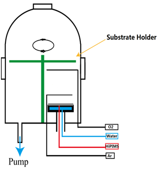
The ZnO films are prepared by HiPIMS on glass substrates at room-temperature(RT), 200°C, 250°C, 280°C, 300°C and 360°C, respectively. Before mounted on the holder, the glass substrates are cleaned in ultrasonic bath with de-ionized water and ethanol for 15 minutes, respectively, and then dried by nitrogen (99.99% in purity) stream. The Zn (99.9999%) target is 9.5cm in diameter and 5 mm in thickness. The distance from target to ring tube of Ar (99.99% in purity) inletting is 4.0 cm, while it is 6.0 cm for O2 (99.999% in purity), and another 3.5cm above O2 ring tube for substrates as Figure 1 shows. The chamber is evacuated to a base pressure of 1.5 × 10⁻³ Pa. The working pressure is maintained at 0.5 Pa by mixed 80 sccm Ar with 16 sccm oxygen. The pulsed voltage, pulsed frequency and pulsed width are set at 800V, 50 Hz, 70 μs, respectively, during ZnO deposition. In the high-power density mode the sputtering peak power is 25 kW and the sputtering peak current is 32A.
Figure 1: The schematic of the experimental setup.
Thickness of as-deposited film is measured by surface profiler (Dektak 150, Veeco). The crystalline of ZnO films is probed by X-Ray Diffraction (XRD) spectroscope (Rigaku) with Cu-Kα source. The surface morphologies of films are characterized by Atomic Force Microscope (AFM) in tapping mode (DI INNOVA, Veeco) and Scanning Electron Microscope (SEM, HITACHI SU8020). The electrical resistivity, mobility, and carrier concentration are detected by Hall Effect equipment (ECOPIA, HMS-3000) at room temperature.
Results and Discussion
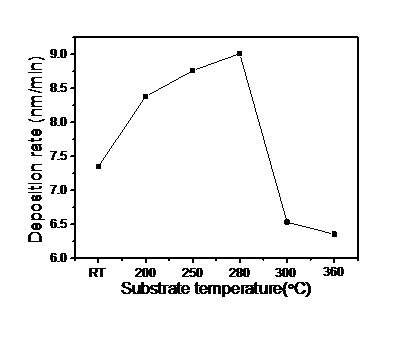
In order to avoid the influence from the film thickness, all films are prepared in similar thickness of 200 ± 20 nm. Figure 2 shows that the deposition rate of ZnO film is 7.35 nm/min at RT, increasing to 9.01 nm/min at 280°C and then decreasing to 6.35 nm/min at 360°C. The increase of deposition rate along with the deposition temperature is owing to the increased kinetic energy of the adsorbed adatom on the substrate surface, which leads to the increase of diffusion length and the enhancement of the condensation between atoms. At further high temperature the decrease of deposition rate is due to the increase of thermal scattering and the reduce of absorption[23]. The reduction of microvoids and pinholes at high temperature, on the other hand, may be one of another reasons to decrease the thickness[29].
Figure 2: Deposition rate of ZnO thin films versus the substrate temperature.
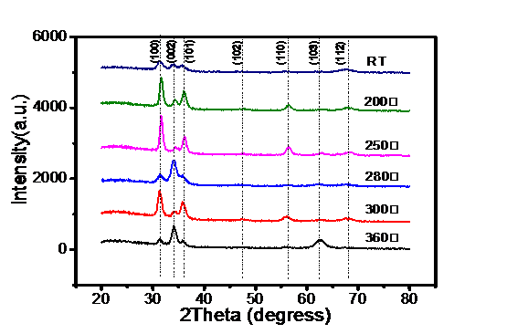
The XRD patterns of ZnO films deposited on glass substrates at different temperatures are shown in Figure 3. The presence of the diffraction peaks indicates that the films are polycrystalline structure, which can be characterized as a wurtzite structure based on JCPDS card 89 - 1397.
Figure 3: XRD patterns of ZnO at different deposition temperatures.
For the sample grown at RT, all weak peaks of wurtzite ZnO at (100), (002), (101) and (112) appears in the pattern. When the samples are grown at high temperature, not only the intensities of peaks are varying, for example, peak at (100) is higher than that at peaks of (002), (101), (110) and (112), but also the patterns are changed. When the deposition temperatures are 250°C and 300°C ZnO films are preferentially grown at the (100) plane[30]. While the deposition temperatures are 280°C and 360°C ZnO films are preferentially grown in (002) facet. This may be the reason that the deposition rate at 280°C is higher and the competition growth between (002) and (103) facets may affect the deposition rate at 360°C.
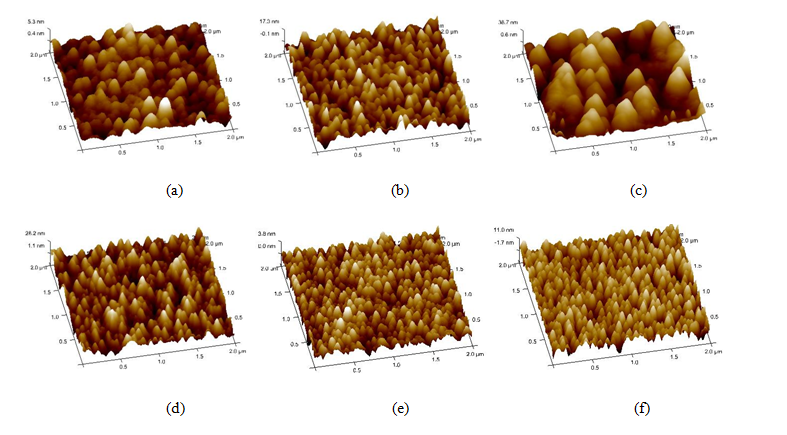
Thermal effect also determines surface morphology and the surface roughness[31]. Figure 4 shows AFM images (2 × 2 μm²) of ZnO thin films grown at the different deposition temperatures. Ra, the average surface roughness, increases from 1.07 nm at room temperature, to 9.85 nm at 250°C and decreases to 0.885 nm at 300°C, and then increases to 2.7 nm at 360°C. It is consistence with the crystal size shown by XRD patterns in Figure 3. At a low temperature, the mobility of adsorbed adatoms on the substrate surface is slow; the film is in amorphous with polycrystalline. At 300°C deposition temperature, the total polycrystalline structure is formed, Ra is smallest than another thin film. The improvement of ZnO surface smoothness may reduce the oxygen adsorption, which leads to a better electrical properties[32]. The roughness increases at 360°C is due to the (002) peak becomes prominent.
Figure 4: AFM images (2 × 2 μm²) of ZnO films at different deposition temperatures ((a) RT, Ra = 1.07 nm; (b) 200°C, Ra = 3.76 nm; (c) 250°C, Ra = 9.85 nm; (d) 280°C, Ra = 6.46 nm; (e) 300°C, Ra = 0.885 nm; (f) 360°C, Ra = 2.7 nm)
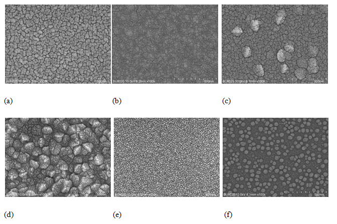
Figure 5 shows the SEM images of the ZnO thin films grown at the six different temperatures. One can see that the surface morphology of the ZnO thin films are changed significantly with the deposition temperatures. Figure 5(a) reveals that ZnO films deposited at RT consists of grains with voids. It is attribution to the fact that the small kinetic energy and the short diffusion path of sputtered adatoms at the low deposition temperatures[22]. When ZnO thin films is deposited at 200°C, Figure 5(b) reveals that the film is more compact. When the deposition temperature is above 250°C, the coalescence of relatively tiny grains forms big crystals as showed in Figure 4(c) and (d), the surface is then rough. When the film is deposited at 300°C a compact structure with small uniform particles is grown as Figure 5(e) shows. It is because of the total polycrystalline ZnO formation at this temperature. At 360°C some bigger grains are grown owing to (002) preferential growth, as showed in Figure 5(f).
Figure 5: The SEM images of ZnO thin films deposited at various growth temperatures. (a) RT; (b) 200°C; (c) 250°C; (d) 280°C; (e) 300°C; (f) 360°C.
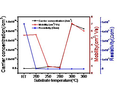
In Figure 6 we obtain that the resistivity of the as-deposited films decreases rapidly from 4.8 × 10³ to 9.29 × 10⁻³ Ωcm with the increase of substrate temperatures from RT to 300°C, and slightly increase at 360°C. In contrary, the carrier concentration of as-deposited films increases along with the temperatures from RT to 300°C, and slightly decreases at 360°C. At 300°C, the carrier concentration of as-deposited ZnO reaches the maximum value of ca. 9.47 × 1019 cm-3. The highest mobility value of 7.1 cm²/Vs is also appeared at 300°C. Generally in ZnO, the equilibrium pressure of oxygen atom is higher than that of zinc atom[33], the high temperature makes the oxygen atoms dissociate from ZnO films easily. As a result, the oxygen vacancies in films increase as the substrate temperature increasing[34]. The more oxygen defects will cause the increase of carrier concentration gradually. When the deposition temperature is 360°C, because the ZnO crystal structure tends to be preferential, the defects are few[33]. Besides, the increasing surface roughness will promotes oxygen absorption and form dangling bonds, which act as electron traps[35]. These electron traps are responsible for the decrease of carrier concentration and carrier mobility.
Figure 6: The relationship of resistivity, carrier concentration and mobility of prepared ZnO films with the deposition temperature.
Conclusion
The role of the deposition temperature on properties of ZnO thin films grown by HiPIMS was investigated in this work. The deposition rate of ZnO films increased from 7.35 nm/min at room temperature, to 9.01 nm/min at 280°C and decreased to 6.35 nm/min at 360°C. The AFM and SEM images indicated that the surface morphology was also dependent on the deposition temperature. AFM images indicated that the Ra of the ZnO thin film deposited at 300°C was smallest; SEM images revealed a compact structure with particles of uniform size formed at 300°C. Hall Effect measurement indicated that ZnO films have a high carrier concentration, a high mobility, and a low resistivity at 300°C. We then conclude that the deposition rate, surface morphology and electrical properties of ZnO films are closely correlated to the substrate temperature.
Acknowledge:
Project supported by the National Natural Science Foundation of China (Grant Nos. 50875132, 60573172), Beijing Municipal National Science Foundation (Grant Nos. 4162024, KZ201510015014, KZ 04190116009/001, KM201510015009, KM201510015002), State Key Laboratory of Electrical Insulation and Power Equipment (No. EIPE15208), the collaborative innovation center of green printing & publishing technology (No. 20160113).
References
- 1. Khomyak, V.V., Ilashchuk, M.I., Parfenyuk, O.A., et al. Fabrication and electrical characterization of the anisotype n-ZnO/p-CdTe heterostructures for solar cell applications. (2013) J Appl Phys 114(22): 223715-223716.
Pubmed || Crossref || Others - 2. Jee, S.W., Park, S.J., KIM, J., et al. Efficient three-dimensional nanostructured photoelectric device by Al-ZnO coating on lithography-free patterned Si nanopillars. (2011) Appl Phys Letters 99(5): 053118-053120.
Pubmed || Crossref || Others - 3. Takada, Y., Okamoto, N., Saito, T., et al. Al: ZnO top electrodes deposited with various oxygen pressures for ferroelectric (Pb, La) (Zr, Ti)O3 capacitors. (2015) Electron Letters 52(3): 230-232 .
Pubmed || Crossref || Others - 4. Mang A., Reimann, K., Rubenacke, St. Band gaps, crystal-field splitting, spin-orbit coupling, and exciton binding energies in ZnO under hydrostatic pressure. (1995) Solid State Commun 94(4): 251-254.
Pubmed || Crossref || Others - 5. Reynolds, D.C., Look, D.C., Jogai, B. Optically pumped ultraviolet lasing from ZnO. (1996) Solid State Commun 99(12): 873-875.
Pubmed || Crossref || Others - 6. Znaidi, L., Touam, T., Vrel, D., et al. AZO Thin Films by Sol-Gel Process for Integrated Optics. (2013) Coatings 3(3): 126-139.
Pubmed || Crossref || Others - 7. Shimizu, M., Shiosaki, T., Kawabata, A. Growth of c-axis oriented ZnO thin films with high deposition rate on silicon by CVD method. (1982) J Crystal Growth 57(1): 94-100.
Pubmed || Crossref || Others - 8. Haga, K., Kamidaira, M., Kashiwaba, Y., et al. ZnO thin films prepared by remote plasma-enhanced CVD method. (2000) J Crystal Growth 214-215: 77-80.
Pubmed || Crossref || Others - 9. Park, S.H., Chang, J.H., Minegishi, T., et al. Investigation on the ZnO: N films grown on (0001) and (0001¯) ZnO templates by plasma-assisted molecular beam epitaxy. (2009) J Crystal Growth 311(7): 2167-2171.
Pubmed || Crossref || Others - 10. Wang, H.C., Liao, C.H., Chueh, Y.L., et al. Synthesis and characterization of ZnO/ZnMgO multiple quantum wells by molecular beam epitaxy. (2013) Opt Mat Express 3(2): 237-247.
Pubmed || Crossref || Others - 11. Naouar, M., Ka, I., Gaidi, M., et al. Growth, structural and optoelectronic properties tuning of nitrogen-doped ZnO thin films synthesized by means of reactive pulsed laser deposition. (2014) Mat Res Bulletin 57: 47-51.
Pubmed || Crossref || Others - 12. Kunj, S., Sreenivas, K. Defect free C-axis oriented zinc oxide (ZnO) films grown at room temperature using RF magnetron sputtering. (2016) AIP Conference Proceedings 1731(1): 080048-1 - 080048-3.
Pubmed || Crossref || Others - 13. Lee, H.B., Hj Jumali, M.H., Ginting, R.T., et al. Mechanistic study on highly crystalline (002) plane bounded ZnO nanofilms prepared via direct current magnetron sputtering. (2015) Mat Letters 161: 83-88.
Pubmed || Crossref || Others - 14. Gobbiner, C.R., Ali Avanee Veedu, M., Kekuda, D. Influence of oxygen flow rate on the structural, optical and electrical properties of ZnO films grown by DC magnetron sputtering. (2016) Appl Phys A 122(4): 272.
Pubmed || Crossref || Others - 15. Duygulu, N.E., Kodolbas, A.O. Investigation of DTS effect on r.f. magnetron sputtered ZnO thin films. (2016) Crystal Res and Technol 51(3): 189-196.
Pubmed || Crossref || Others - 16. Ahmad, A.A., Alsaad, A.M., Albiss, B. A., et al. The effect of substrate temperature on structural and optical properties of D.C. sputtered ZnO thin films. (2015) Physica B Condensed Matter 470-471: 21-32.
Pubmed || Crossref || Others - 17. Subramanyam, T.K., Naidu, B.S., Uthanna, S. Effect of substrate temperature on the physical properties of DC reactive magnetron sputtered ZnO films. (1999) Optical Materials 13(2): 239-247.
Pubmed || Crossref || Others - 18. Singh, S., Srinivasa, R.S., Major, S.S. Effect of substrate temperature on the structure and optical properties of ZnO thin films deposited by reactive rf magnetron sputtering. (2007) Thin Solid Films 515(24): 8718-8722.
Pubmed || Crossref || Others - 19. Chaabouni, F., Abaab, M., Rezig, B. Effect of the substrate temperature on the properties of ZnO films grown by RF magnetron sputtering. (2004) Materials Sci Eng: B 109(1–3): 236-240.
Pubmed || Crossref || Others - 20. Cho, S.H. Effects of Growth Temperature on the Properties of ZnO Thin Films Grown by Radio-frequency Magnetron Sputtering. (2009) Transactions on Electrical & Electronic Materials 10(6): 185-188.
Pubmed || Crossref || Others - 21. Xianwu, Yuping, Zhiyong, et al. Effects of Substrate Temperature on the Properties of Mo-doped ZnO Films Prepared by RF Magnetron Sputtering. (2009) J Materials Sci Technol 25(6): 785-788.
Pubmed || Crossref || Others - 22. Huang, J., Tan, R., Zhang, Y., et al. Effects of substrate temperatures on the thermal stability of Al-doped ZnO thin films grown by DC magnetron sputtering. (2012) J Materials Sci: Materials in Electronics 23(2): 356-360.
Pubmed || Crossref || Others - 23. Wang, J., Sallet, V., Jomard, F., et al. Influence of substrate temperature on N-doped ZnO films deposited by RF magnetron sputtering. (2007) Thin Solid Films 515(24): 8785-8788.
Pubmed || Crossref || Others - 24. Bohlmark, J., Alami, J., Christou, C., et al. Ionization of sputtered metals in high power pulsed magnetron sputtering. (2005) J Vacuum Sci Technol A: Vacuum, Surfaces, and Films 23(1): 18-22.
Pubmed || Crossref || Others - 25. Kouznetsov, V., Mac, K.K., Schneider, J.M., et al. A novel pulsed magnetron sputters technique utilizing very high target power densities. (1999) Surface & Coatings Technol 122(2-3): 290-293.
Pubmed || Crossref || Others - 26. Vlček, J., Kudl Ček, P., Burcalov, K., et al. High-power pulsed sputtering using a magnetron with enhanced plasma confinement. (2007) J Vacuum Sci Technol A Vacuum Surfaces & Films 25(1): 42-47.
Pubmed || Crossref || Others - 27. Kudlacek, P., Vlček, J., Burcalov, K., et al. Highly ionized fluxes of sputtered titanium atoms in high-power pulsed magnetron discharges. (2008) Plasma Sources Sci & Technol 17(2): 025010-1 - 025010-8.
Pubmed || Crossref || Others - 28. Gupta, R., Pandey, N., Behera, L., et al. Study of cobalt mononitride thin films prepared using DC and high power impulse magnetron sputtering. (2016) 1731(1): 3348-2944.
Pubmed || Crossref || Others - 29. Ghosh, S.P., Das, K.C., Tripathy, N., et al. Morphological evolution of zinc oxide thin films with variation in sputtering power and substrate temperature. (2016) Int J Microstructure & Materials Properties 11(5): 325-338.
Pubmed || Crossref || Others - 30. Othmane, M., Attaf, A., Saidi, H., et al. Modulation of Physical Properties of Sprayed ZnO Thin Films by Substrate Temperature for Optical Applications. (2016) Int J Nanosci 15(1): 1650007-1 - 1650007-8.
Pubmed || Crossref || Others - 31. Cheng, J., Hu, R., Wang, Q., et al. Substrate Temperature Effect on Charge Transport Performance of ZnO Electron Transport Layer Prepared by a Facile Ultrasonic Spray Pyrolysis in Polymer Solar Cells. (2015) Int J Photoenergy 201472-1 - 201472-8.
Pubmed || Crossref || Others - 32. Sin, N.D.M., Ahmad, S., Musa, M.Z., et al. Structure transformation of ZnO thin films properties influenced by substrate temperature deposited by magnetron sputtering. (2012) proceedings of the Humanities, Science and Engineering Research 431-435.
Pubmed || Crossref || Others - 33. Li, X.H., Zhu, M.K., Hou, Y.D., et al. Influence of Substrate Temperature on Oxygen Defects of ZnO Thin Films. (2004) Piezoelectrics & Acoustooptics 26(4): 318-320.
Pubmed || Crossref || Others - 34. Zhang, C., Chen, X.L., Geng, X.H., et al. Temperature-dependent growth and properties of W-doped ZnO thin films deposited by reactive magnetron sputtering. (2013) Appl Surface Sci 274: 371-377.
Pubmed || Crossref || Others - 35. Moon, Y.K., Kim, S.H., Park, J.W. The influence of substrate temperature on the properties of aluminum-doped zinc oxide thin films deposited by DC magnetron sputtering. (2006) J Materials Sci: Materials in Electronics 17(12): 973-977.
Pubmed || Crossref || Others


