Investigating the Properties of Indium-Free Amorphous Oxide Semiconductor Films for Potential TFT Application on Flexible Substrates
Robert Alston1, Jia Li1 and Shanthi Iyer1,2*
Affiliation
- 1Department of Electrical and Computer Engineering, North Carolina Agricultural & Technical State University, Greensboro, NC, USA
- 2Department of Nanoengineering, North Carolina Agricultural & Technical State University, Greensboro, NC, USA
Corresponding Author
Shanthi Iyer, Department of Electrical and Computer Engineering, North Carolina Agricultural & Technical State University, Greensboro, NC, USA 27411. E-mail: sni0124@gmail.com
Citation
Shanthi, I., et al. Investigating the Properties of Indium-Free Amorphous Oxide Semiconductor Films for Potential TFT Application on Flexible Substrates (2014) J Nanotech Mater Sci 1(1): 7-11.
Copy rights
© 2014 Shanthi I. This is an Open access article distributed under the terms of Creative Commons Attribution 4.0 International License.
Keywords
RF-sputtered gallium tin zinc oxide; Polyethylene naphthalate; AMLCD
Abstract
RF-sputtered gallium tin zinc oxide (GSZO) thin fims for application in transparent amorphous oxide semiconductors (TAOSs) have been investigated. Morphological, structural, electrical, optical properties and its mechanical robustness have been studied on polyethylene naphthalate (PEN) substrates using variety of characterization techniques. The fims deposited on PEN substrates retained amorphous structure even after annealing for 12 hours in vacuum at 200°C. The optical band edge is ~ 3.3eV, greater than ZnO fims. Best μHall of 3 cm²V- 1s- 1 have been observed on annealed GSZO fims at 200°C. The critical radii of bending improve from 14.5 mm to 11 mm with decreasing RF power of deposition from 90W to 80W, indicative of its suitability for flxible electronics.
Introduction
Signifiant strides have been made in the development AOS thin film transistor (TFT) device research in the last few years leading to current widespread applications as switching transistors in the back plane array for high definition flt panel display (FPD) applications, particularly in active matrix liquid crystal displays (AMLCD).The enhanced research in AOS began with the demonstration of amorphous indium gallium zinc oxide (IGZO) TFTs by Nomura et al[1] in 2004. Despite the amorphous state, the IGZO channel exhibited high mobility due to the overlap of the adjacent ns orbitals. The spherical symmetry of the orbital’s renders the material less prone to structural deformation on bending and is a promising material system for flexible electronics applications.
Amongst AOSs IGZO TFTs have been the extensively studied[2-4] due to its superior electrical characteristics such as low sub-threshold swing (SS) < 0.5 V/dec and μFE exceeding 20 cm2/V°s, along with high optical transparency and low-temperature fabrication process[5]. However the scarcity of indium and associated high cost have provided the impetus to the research of a replacement material[6]. The extensively researched electrical properties of IGZO have set a high standard for replacement alloys. Promising alternate wide band gap (3.2 eV) ZnO based alloy systems without In that have been ex-amined are zinc gallium oxide (ZGO), zinc tin oxide (ZTO) and gallium tin zinc oxide (GSZO). Amongst these, GSZO is more attractive due to the similar electronic configuration [Kr]5s0 of Sn4+ and In3+ and potential of comparable TFT performance at low temperatures[7]. Further the composition of GSZO consists of smaller amounts of expensive element Ga in comparison to those in IGZO alloys.
Fortunato et al[6]. Reported on electrical characteristics of GSZO films and the TFTs. TFTs with GSZO channel layers RF-sputtered at room temperature were compared to TFTs with channel layers deposited at 150°C. The resistivity of as - deposited GSZO films decreased by 8 orders of magnitude from 4.6x10¹⁰ Ω°cm to 10² Ω°cm after annealing at 250°C. Room temperature deposited GSZO TFTs exhibit a Vth of 6.5 V and Ion/off of 6x10⁷ after being annealed at 300°C. GSZO TFTs with channel layers deposited at 150°C exhibited improved output characteristics with Vth of 4.6V and Ion/off of 8x10⁷ after being annealed at 300°C. Recently, Bradley et al[7] reported significant lowering of the annealing temperature from 300°C to 150°C to achieve similar performance Vth = -2.5 V and Ion/off = 2x10⁶ while increasing the deposition temperature to a modest value of 50°C. A stable device was achieved with shifts in V th as low as ~0.5 V for 3hr stress under a gate bias of 1.2 and 12 V along with good optical stability. Thus suitable tuning of the deposition and annealing parameters were shown to lead to a very stable device both optically and electrically.
Thus the GSZO based TFTs appear to be promising and in this work we report on our preliminary investigation of properties of GSZO films with a view to implement on flexible substrates. Morphological, structural, electrical and optical properties of the layers are examined on both 7059 glass and polyethylene naphthalate (PEN) substrates using variety of characterization techniques. The mechanical robustness of the films was compared to our earlier work[8] on the RF sputtered ZnO:F films.
Materials and Methods
The sputtering system used to deposit films in our investigative process was the Edwards ESM Sputtering Tool with a GSZO target. Depositions were conducted at room temperature in an Ar/O2 gaseous combination of 100/2 sccm and the thickness of the films deposited was 30 nm unless otherwise specified on glass and on 200 μm thick DuPont Teonex® Q65 PEN substrates. The films were annealed at 200°C in air for different durations for all the characterization except for electrical characteristics. In this case the annealing was carried out in rough vacuum as air annealing resulted in large increase in resistivity which prevented in carrying out the conventional Hall measurement as discussed below. Electrical measurements were performed using a Varian Hall effect measurement system using magnetic fields of 0.8T and the van der Pauw configuration. The surface morphology of as-deposited and annealed films was studied using the NanoScope III Dimension 3100 atomic force microscopy (AFM) system. X - ray diffraction (XRD) was performed using a Bruker AXS Discover series XRD to analyze the film crystallinity of as-deposited and various annealed films deposited on PEN and 7059 glass substrates.
Transmission measurements were carried out using a Varian/Agilent 670 FTIR spectrometer. The absorption spectra were determined from the respective transmission and reflection spectra. The absorption coefficient, α, of the respective films were extracted from these two data using Beer-Lambert law. The optical gap was determined from the following Equation (1) by extrapolating the linear part of the α2 vs. energy plot.
α(hυ) =(hυ-Eg)(1/2) (1)
Bend test measurements were taken to calculate the critical radius of GSZO films deposited under different conditions. Bend testing of the samples was carried out using a collapsing radius system built in-house wherein the films were held between two flat parallel figures. The films are then gradually collapsed in a cylindrical configuration from a maximum to the desired radius 'r' by moving one of the mobile figures. The automated system consisted of a mechanical translation stage integrated with the sample figure that logs electrical data from an external digital multi meter. The experiments were performed with the film on the outer bend surface of PEN substrate such that it undergoes tensile strain. Finally, Nomarski microscope images were taken of the bend - tested GSZO films on PEN to examine the structural deformation of the film.
Results and Discussion
Atomic Force Microscopy
AFM images were taken of 30 nm GSZO films deposited on silicon and annealed for 1 and 8 hours (Figure 1(a) and Figure 1(b)).The depth distribution on these images has been computed from the variation of surface points in reference to the average surface level. The GSZO film exhibits a relatively smooth surface morphology corresponding to a RMS roughness of 4.72° when annealed for 1 hour duration. With increasing annealing duration to 8 hours the AFM images show an increase in surface roughness to 25.3°. This increase in surface roughness is speculated to be attributed to the absorption of oxygen and/or water molecule from air.
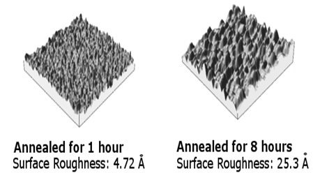
Figure 1(a) : AFM images of GSZO films annealed for 1 hour.
Figure 1(b) : AFM images of GSZO films annealed for 8 hours.
X - ray Diffraction
XRD results performed on films deposited onto 7059 glass and annealed for durations of 8 and 12 hours along with a bare un - annealed 7059 glass substrate are shown in Figure 2.
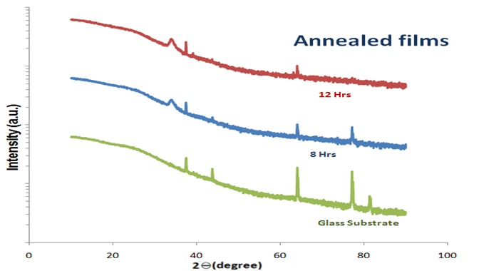
Figure 2: XRD spectra of GSZO films deposited on glass substrates and GSZO films deposited on glass and annealed for 8 and 12 hours.
The short spikes observed in both the glass and PEN graphs (shown in Figure 3) are a result of the stage on which the samples were fastened for characterization. A small peak at 30° for the 8 hours annealed films suggests the onset of crystallinity in these films.
XRD results of as-deposited films on PEN substrate and subsequently annealed for 8 and 12 hours along with a reference bare PEN substrate are shown in Figure 3. There is no observable difference in the full width half maxima of the peaks between the bare PEN substrate and the annealed samples. These results indicate that the films deposited on PEN substrates retain the amorphous state.
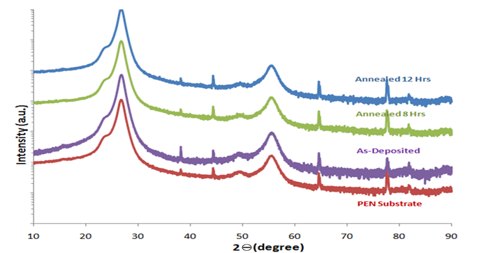
Figure 3: XRD spectra of a bare PEN substrate, GSZO as-deposited films and films annealed for 8 and 12 hour duration.
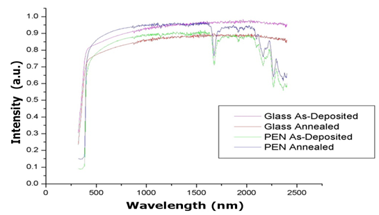
Figure 4 illustrates transmission measurements conducted on GSZO as - deposited and annealed films deposited on PEN and glass. The variation of the absorption edges of the GSZO films with energy are shown in Figure 5. These samples are compared to corresponding ZnO:F as - deposited films on those two substrates. Optical band gap of GSZO was found to be around 3.3eV, larger than ZnO:F, resulting in a more transparent film. As - deposited GSZO films on glass exhibited slightly smaller energy band gap than annealed one, contrary to the observation on the PEN substrate. However, it is to be noted that these shifts are within the margin of experimental error.
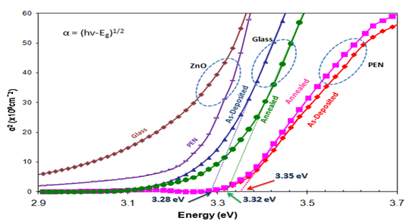
Figure 5: Energetic dependence of α2for as-deposited and annealed GSZO and ZnO films on glass and pen substrates.
Electrical Characteristics
Figures 6-8 exhibit the variation of resistivity, ρ carrier concentration, n, and Hall mobility, μ Hall, of GSZO films deposited on glass with annealing duration for different sputtering powers. The highest resistivity in the film is achieved for the sputtering power of 100 W mainly due to the low carrier concentration. Latter in conjunction with the increased mobility at higher sputtering power suggests that this is largely due to the change in the composition resulting from the plausible difference arising from the sputtering yield of the different components and local atomic arrangement, as opposed to the increased surface damages at higher deposition powers.
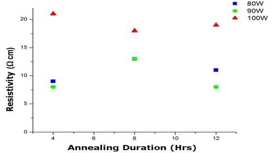
Figure 6: Variation of resistivity in GSZO films deposited on glass with varying annealing durations and deposition powers.
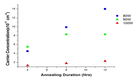
Figure 7: Variation of carrier concentration in GSZO films deposited on glass with varying annealing durations and deposition powers.
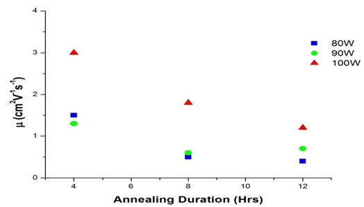
Figure 8: Variation of carrier mobility in GSZO films deposited on glass with varying annealing durations and deposition powers.
The ρ values vary only marginally with annealing duration, the lowest resistivity being 8 Ω°cm. The variation of n and μ Hall with annealing duration exhibit an opposite trend. Further, n increases more rapidly with annealing duration for the GSZO films deposited at 80 W while the carrier mobility decreases more sharply at higher sputtering power. The highest μ Hall of 3 cm2 V-1s-1 was obtained for a carrier concentration of 1017 cm-3 and resistivity of 21 Ω°cm on GSZO films deposited at 100 W and annealed for 4 hours.
An increase in n suggests an increase in oxygen vacancies which may contribute to formation of more donor states. This is consistent with decreasing μ Hall, which is indicative of dominance of ionized impurity scattering limiting the carrier mobility. The opposite trends in these two parameters lead to little variation in the observed resistivity.
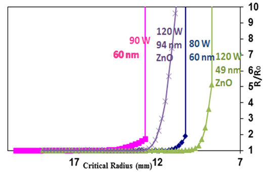
Figure 9 illustrates the results of the bend test measurements performed on GSZO and ZnO films. The GSZO films of 60nm thickness were deposited at 90 W and 80 W, and compared with the ZnO:F films deposited at 120 W with differing thicknesses of 94 and 49 nm. GSZO films were annealed at 200°C for 4 hours while ZnO:F films were annealed in 7% H2/Ar ambient at 150°C for 1 hour. The critical radius was determined to be the radius where the resistance doubles its initial value. R0 is the initial resistance of the film recorded before bending the sample, and R is the resistance measured during the bend process. The films experience a linearly variable strain normal to the direction of the applied stress. In our case the strain varies from compressive on the inside curvature of the substrate to the tensile on the outer surface of the film, with a constant strain in the plane of the film. The dependence of the film strain, εf, on the radius of curvature, r, was computed from a simple relationship below
εf = d /(2 * r) (2)
using conventional beam theory[9], where d is the thickness of the substrates the thickness of the film is neglected. The critical radius of curvature in the 14.5 - 11mm range observed in GSZO films corresponds to strains in the range of ~ 0.70.-0.90%. These are consistent with the typical strains at which micro cracks appear in oxide thin films deposited on flexible substrates[8]. Both the critical radius of the films and the shape of the bending curves are strongly influenced by the wattage of the deposited films as well as the type of the film. From the thickness and sputtering power dependencies shown in the Figure 9, it may be extrapolated that for similar thickness and under similar sputtering power conditions, GSZO films would exhibit much larger critical radii in comparison to ZnO: F films with steeper failure curve. The common cause for the fracture of the film and the loss of electrical conductivity in the films is attributed to the formation and propagation of micro cracks through the film thickness and in plane. These micro cracks may originate from the pin holes in the films, embedded voids from deposition, and/or surface defects from the underlying PEN substrates. The difference in crystallinity exhibited by the two films also contributes to the differences in the observed failure curves. ZnO films are polycrystalline as opposed to the amorphous structure of the oxide films. Films deposited at lower deposition power leads to smaller critical radius consistent with the lower carrier mobility observed in these films, both indicative of somewhat more defective films.
Nomarski Microscope Images
Results of the Nomarski microscope images of the GSZO film with a thickness of 60 nm and annealed at 200°C for 4 hours prior to bending and after bending the film beyond the critical radius are shown in Figure 10.
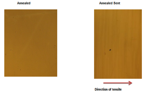
Figure 10: Nomarski microscope images of the GSZO film surface before and after performing bend testing.
The stress lines formed in the annealed bent film is normal to the direction of the tensile stress applied and may be attributed to the amorphous nature of GSZO films and lack of grain boundaries.
Conclusion
In conclusion, in this work we report our results on the structural, electrical, optical properties of RF-sputtered GSZO films. XRD results show that the GSZO films deposited on PEN substrate retains amorphous nature even after annealing at 200°C for 12 hours. The best carrier mobility of 3cm2V-1s-1 were obtained on films exhibiting a ρ of 21 Ω°cm, n of 1017cm-3, which were deposited at 100 W and annealed at 200°C for 4 hours. The films exhibit a higher band gap of 3.3 eV higher than those observed in ZnO films. Bend tests reveal GSZO films show a steeper failure curve than ZnO;F films and exhibit higher critical radii than ZnO films. However the critical radii decreases with wattage of the deposition power and thus demonstrates the potential of GSZO material system for future flexible electronics applications.
Acknowledgement
This work is supported by the Army Research Office (Grant# W911NF-10-1-0316, technical monitor MikeGerhold) and Department of Education Title III program.


